So I finally came about testing the NT1065… apologies for the lack of detail but I have done this in my very little spare time. Also, I would like to clarify that I am in no way affiliated to NTLab.
Chip overview
A picture speaks more than a thousand words.
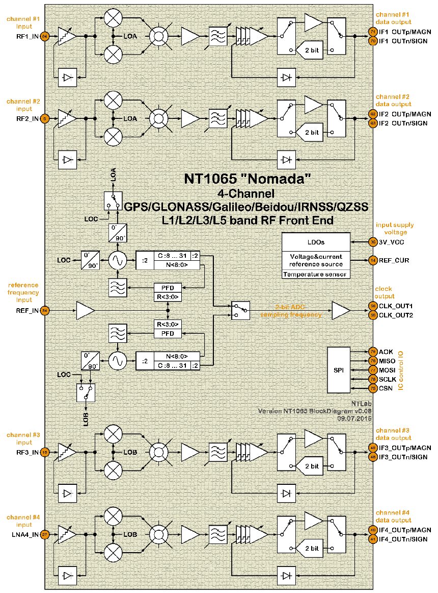
Figure 1: NT1065 architecture
Things worth noting above are:
- Four independent input channels with variable RF gain, so up to 4 distinct antennas can be connected;
- Two LOs controlled by integer synthesizers, one per pair of channels, tuned respectively for the high and low RNSS band, but one can choose to route the upper LO to the lower pair and have 4 phase coherent channels
- ADC sample rate derived from either LO through integer division
- 4 independent image-reject mixers, IF filters and variable gain (with AGC) paths
- Four independent outputs, either as a CMOS two bit ADC or analogue differential so one could
- connect his/her own ADC or
- phase-combine the IF outputs in a CRPA fashion prior to digitisation
- standard SPI port control
Another important point for a hardware designer (I used to be a little bit of that) is this:

Figure 2: NT1065 application schematic
The pin allocation shows a 1 cm2 QFN88 (with 0.4mm pin step) with plenty of room between the pins and an optimal design for easy routing of the RF and IF channels. Packages like that aren’t easy to find nowadays for such complex RF ICs (everything is a BGA or WLCSP) but I love QFNs because they are easy to solder with a bit of SMD practice and can be “debugged” if the PCB layout is not perfect first time.
Evaluation kit overview
The evaluation kit presents itself like this:
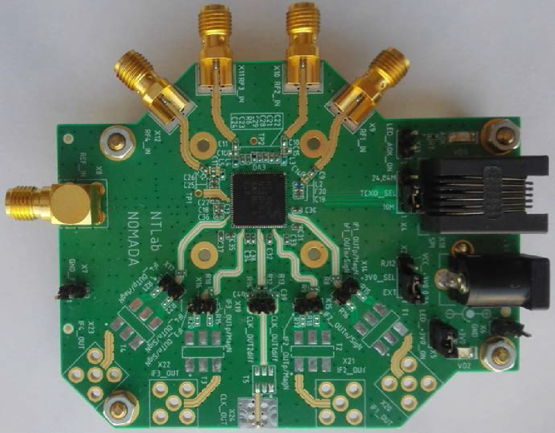
Figure 3: NT1065 evaluation kit
One can see the RF inputs at the top, the external reference clock input on the left, the control interface on the right and the IF/digital part on the bottom. The large baluns (for differential to single ended conversion) were left unpopulated for me as I don’t use redpitaya (yet?). The control board is the same used for the NT1036.
In configured the evaluation kit to be powered by the control board (it was an error, see later) and connected the ADC outputs and clock to the Spartan6 on the SdrNav40, used here simply as USBHS DAQ. In total, there is one clock like and 8 data lines (4 pairs of SIGN/MAGN, one per channel).
The IF filters act on the Lower Side Band (LSB) or the Upper Side Band (USB) for respectively high and low injection mixing and can be configured for a cutoff frequency between 10 and 35 MHz. Thus, bandwidths of up to 30 MHz per signal can be accommodated and the minimum ADC sampling rate should be around 20 Msps. 20 MByte/sec are not easy to handle for a USBHS controller, so I will look into other more suitable (but still cost effective) DAQ options to evaluate the front-end. In the meantime, I could do a lot with 32MByte/sec of the FX2LP by testing either 2 channels only with 2 bit or all the 4 channels with 1 bit and compressing nibbles into bytes (halving the requested rate).
The evaluation software is a single window, very simple and intuitive to use but very effective.
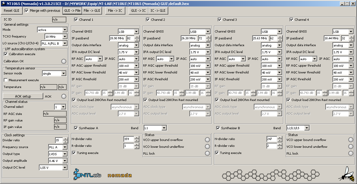
Figure 4: Evaluation software
The software comes with several sample configuration files that can be very useful to quickly start evaluating the chip.
Tests
All my tests used a good 10MHz CMOS reference.
GPS L1
The first test was GPS L1 in high injection mode setting the first LO to 1590 MHz (R1=1, N1=159), leading to an IF of -14.58 MHz, a filter bandwidth of about 28 MHz and a sampling frequency of 53 Msps (K1/2=15). I streamed one minute to the disk and verified correct operation.
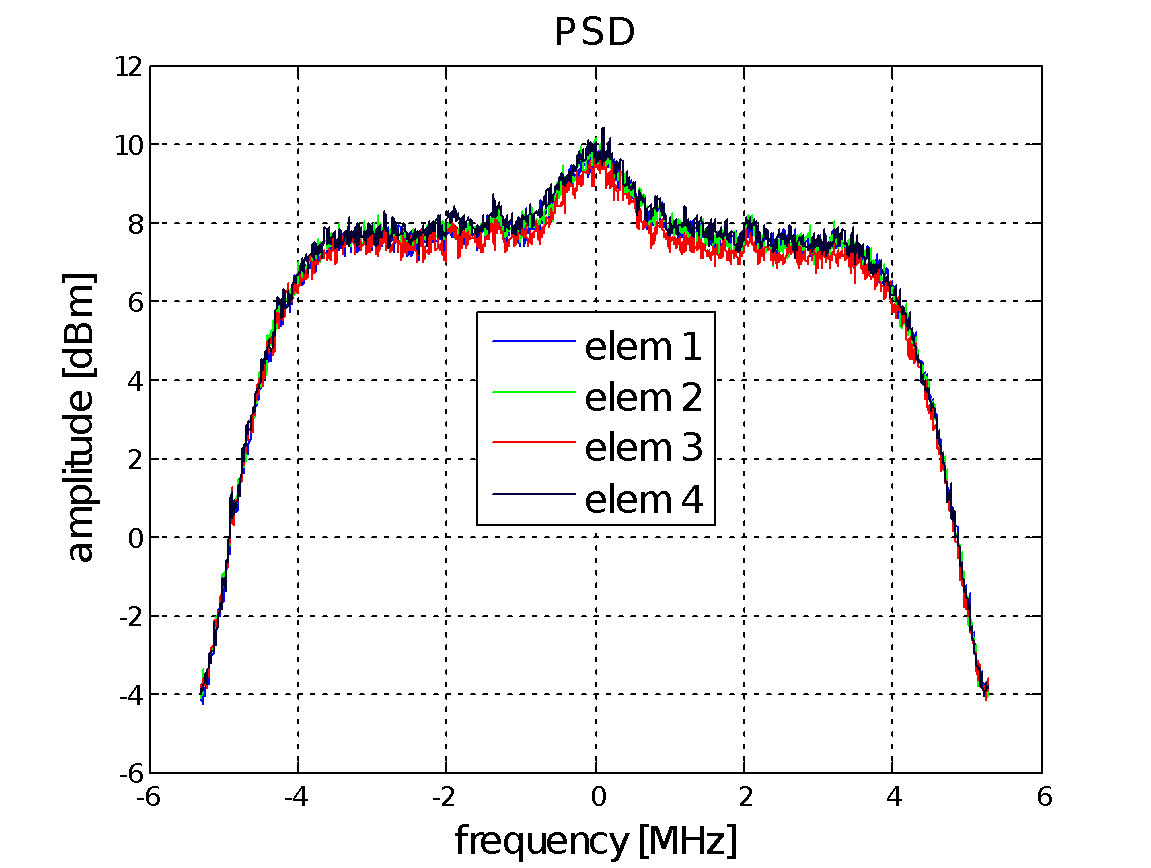
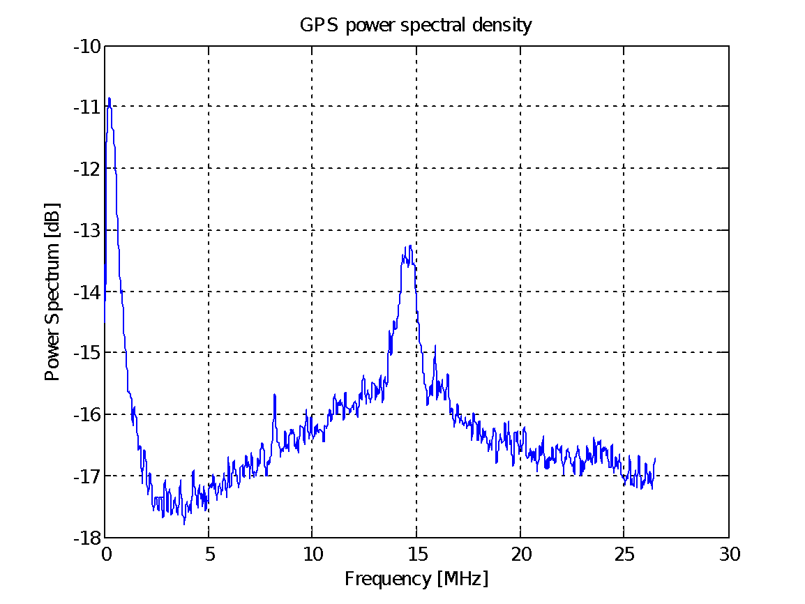 | 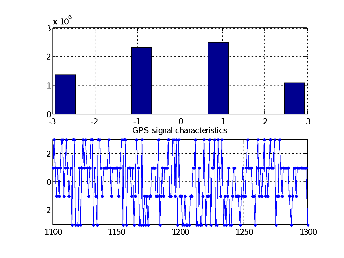 |
Figure 5:GPS L1 PSD (left) and histogram+time series (right)
 | 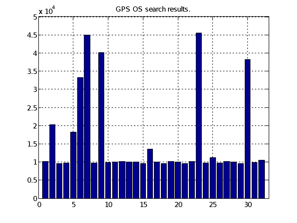 |
Figure 6: G30 correlation of L1 code detail (left) and all satellites (right).
GPS L1/L5
When performing this test I bumped into a hardware problem. If the control board powers the NT1065 evaluation kit with its internal 3.3V reference, the power line is gated by a small resistor thus the voltage depends on the current drawn by the chip (undesirable!). Enabling the second channel in the GUI made the chip draw more current so the voltage on the evaluation kit decreased away from the SdrNav40 one which was steady at 3.3V. Level mismatch created unreliability in reading the digital levels and failure to transfer meaningful data. So I powered the evaluation kit with the SdrNav40 3.3V voltage reference and everything was happy again.
In this configuration L1 is again at -14.58 MHz (1590 MHz high side injection) and L5 is on the third channel (low RNSS) at -13.55 MHz (R2=1, N2=119 for 1190 MHz high side injection). To be noted the relative large spike in the spectrum at 1166 MHz, not an obvious harmonic so it could be some unwanted emission from neighbour equipment.
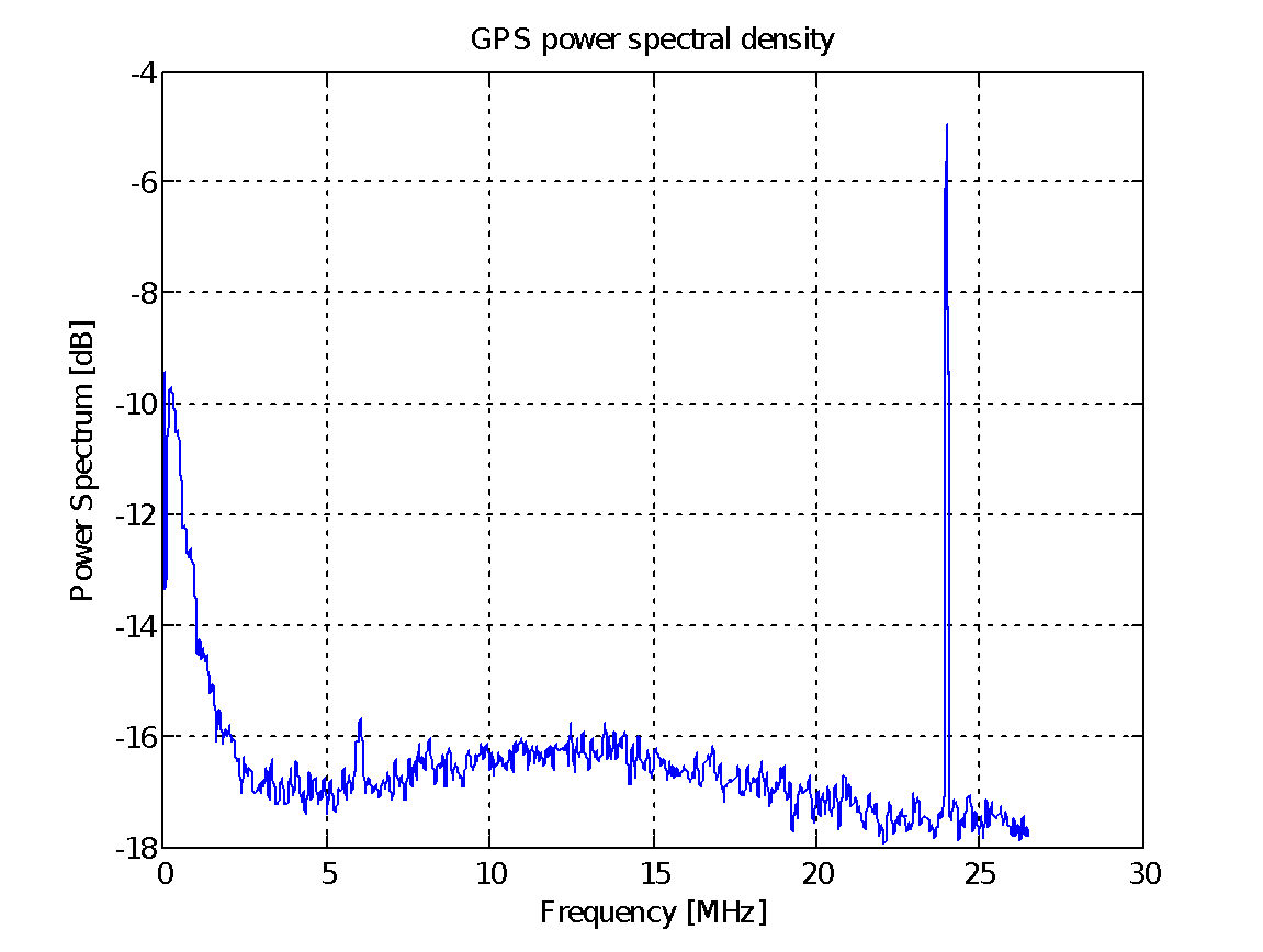 | 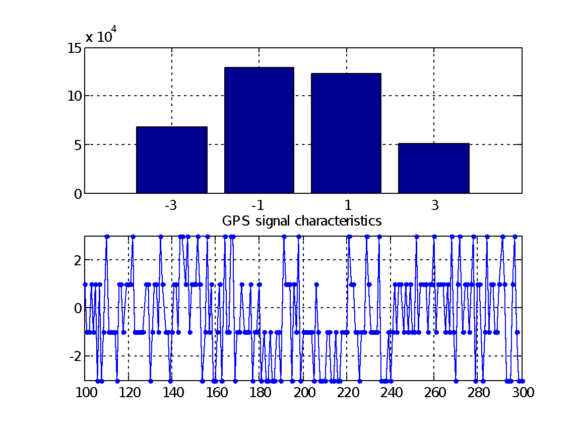 |
Figure 7: L5 PSD (left) and histogram+time series (right)
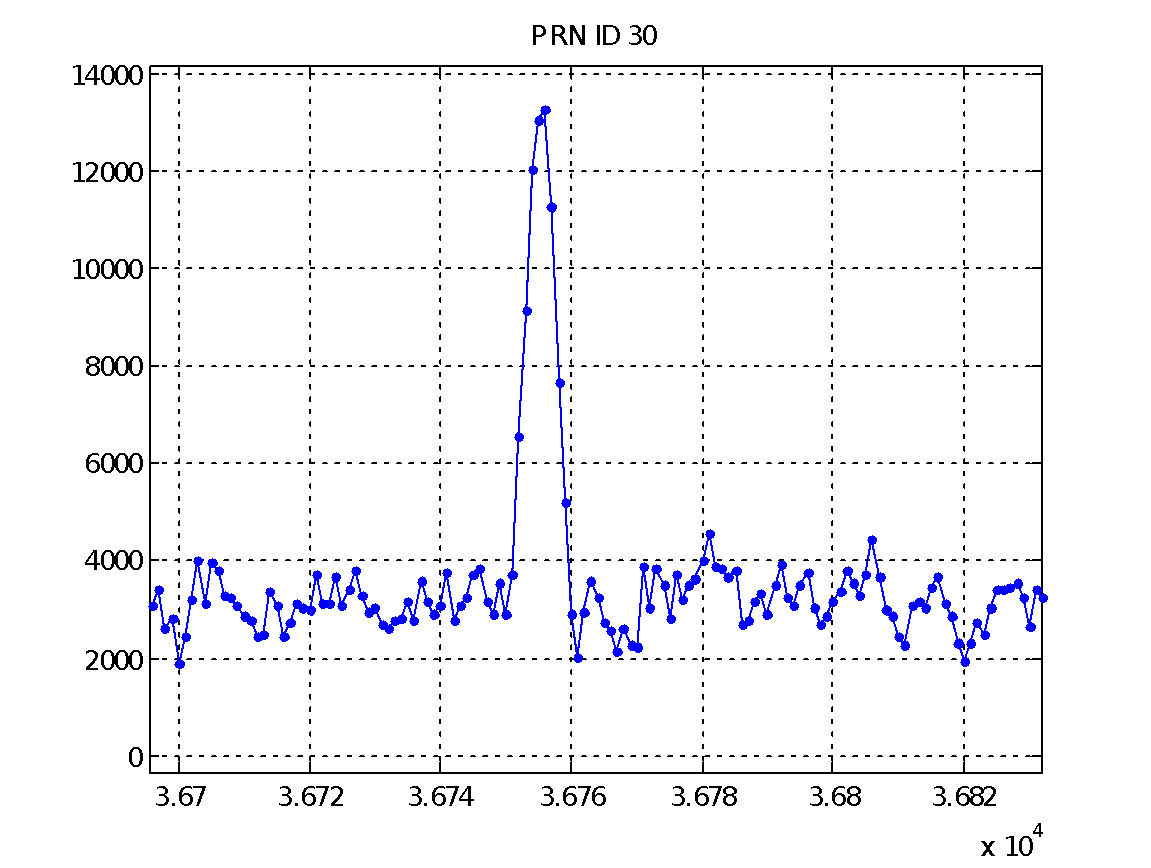 |  |
Figure 8: G30 correlation of L5 code detail (left) and all satellites (right).
Interestingly, the Matlab satellite search algorithm returns respectively for L1 and L5:
Searching GPS30 -> found: Doppler +4500.0 CodeShift: 35226 xcorr: 12502.4
Searching GPS30 -> found: Doppler +3000.0 CodeShift: 35226
The above outputs show coarse but correctly scaled Doppler [Hz] and a perfect match in code delay [samples] (just by chance spot on).
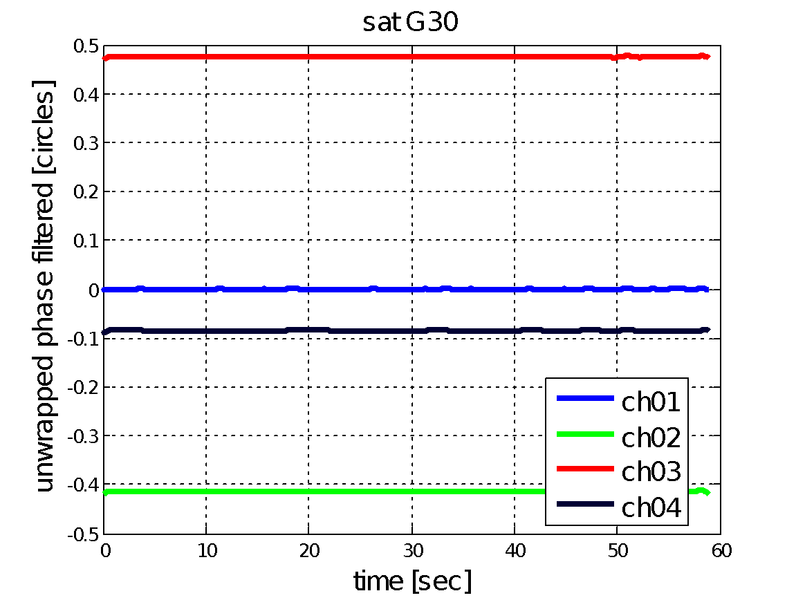
4x GPS L1
In this case I enabled all 4 channels and shared the LO amongst them all. Unfortunately I cannot show the 6dB increase in gain when steering a beam to a satellite as all RF inputs were connected to the same antenna and -being the noise the same- steering the phase is useless. However, it is possible to verify how the phase amongst the channels is perfectly coherent (requirement for an easy CRPA).
The signals were conveniently brought to baseband, filtered and decimated by 5, resulting into a 10.6 MHz sampling rate. As one can see below the power was well matched and the inter-channel carrier phase is extremely steady and constant over the 60 seconds capture time. In the very case of zero-baseline, one can easily check that such phase difference is also the same across different satellites (as it does not depend on geometry but just on different path lengths beyond the splitter).
 |  |
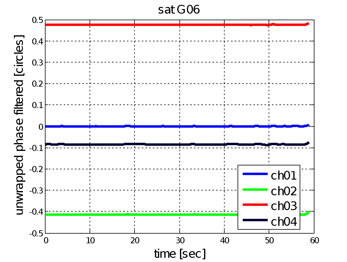 |  |
Figure 9:PSD of the IF obtained from the 4 channels and relative carrier phase
GPS L1 + Glonass G1 + GPS L5 + Glonass G3
I wanted to verify here reception of Glonass G1 on the second channel (upper side band). At this point it had become merely a formality. Glonass CH0 is at +12 MHz so the acquisition returned correctly as shown below. Of course 53 Msps for a BPSK(0.5) is a bit of an overkill :)
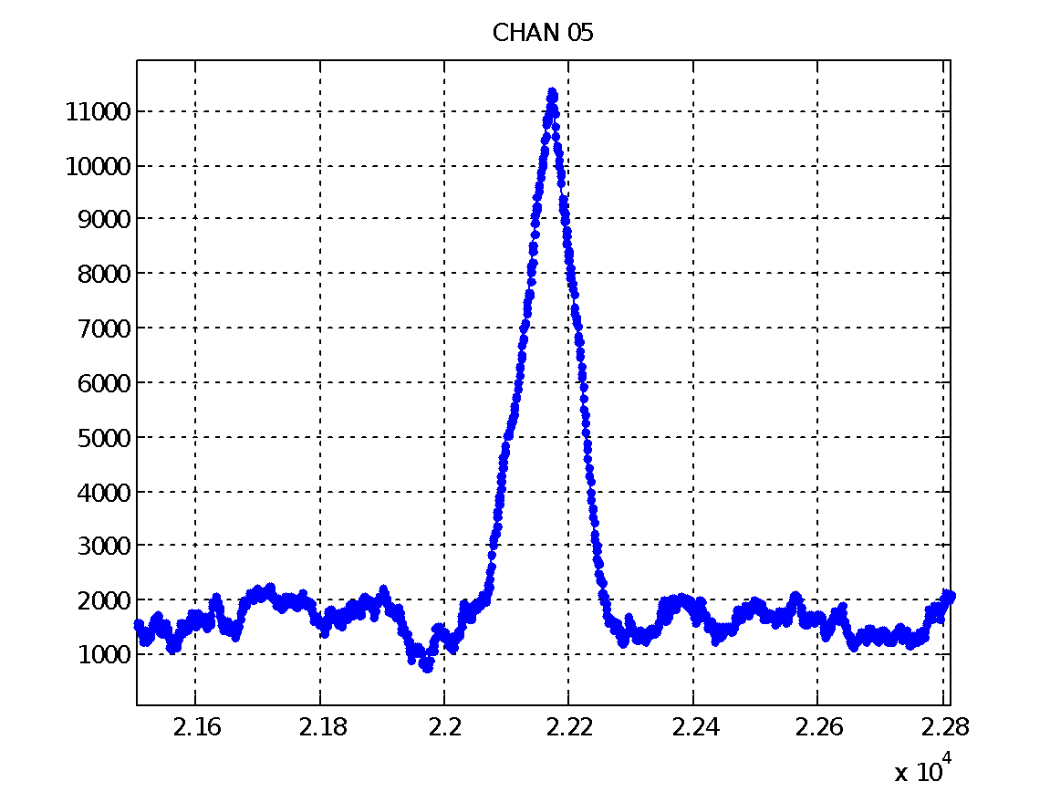 |
Figure 10: Glonass acquisition all satellites (left) and CH-5 detail (right).
GPS L1 + Beidou B1 + GPS L5 + Galileo E5b
The case for GPS and Beidou was a bit more challenging as the distance between L1 and B1 is only 14.322 MHz, thus the IFs must be around 7 MHz. I decided to set the LO to 1570 MHz (R1=1, N1=157). So GPS went upper side band on channel 1 at +5.42 MHz IF. Beidou consequently went on lower side band on channel 2 at -8.902 MHz. Channel 3 and 4 were enabled with LO2 set at 1190 MHz: in the middle between E5a and E5b in order to verify AltBOC reception.
As 1570 MHz is a nasty frequency to generate a round sampling frequency value I decide to derive the clock from LO2 using K2/2 = 10 and therefore stream at 59.5 Msps. As one can see below the L1 peak has moved very close to baseband now and the sampling frequency is quite exceeding the Nyquist limit.
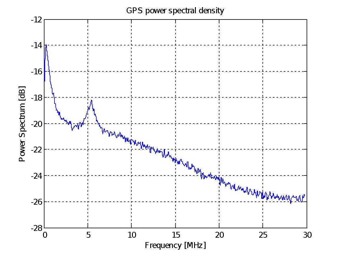 | 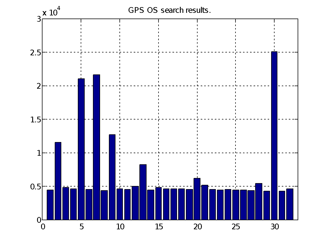 |
Figure 11: GPS acquisition with close-in IF
 |  |
Figure 12: Beidou B1 sprectrum (MSS on the right) and acquisition (incidentally also showing IGSO generation 3 satellites C31 and C32).
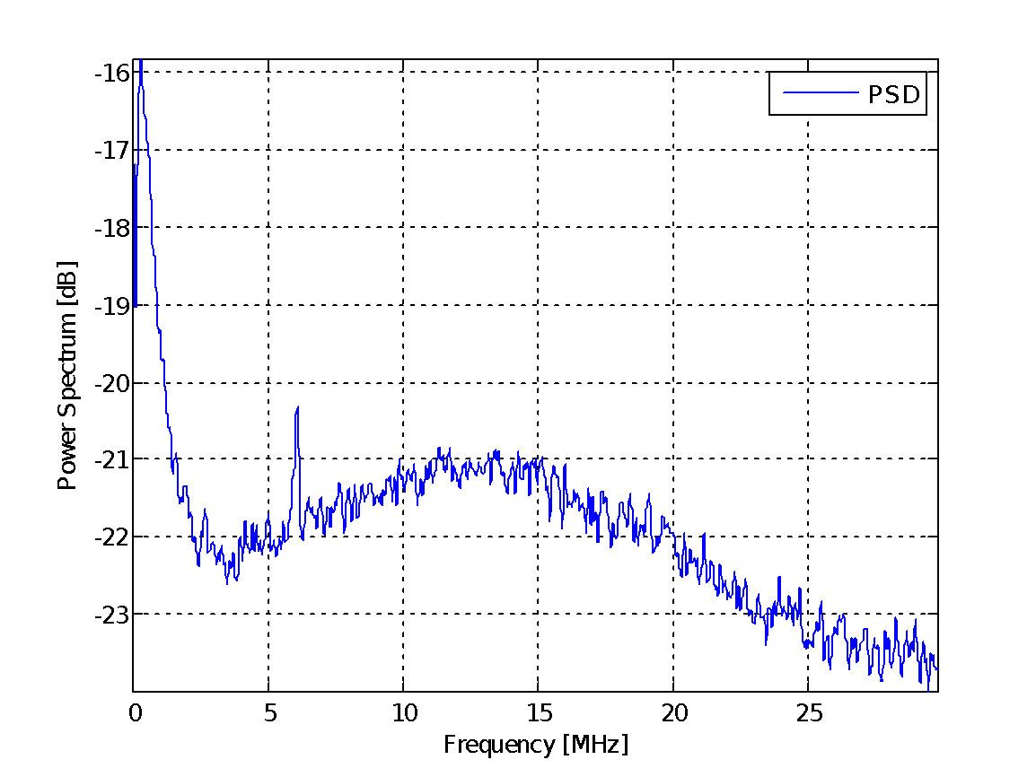 | 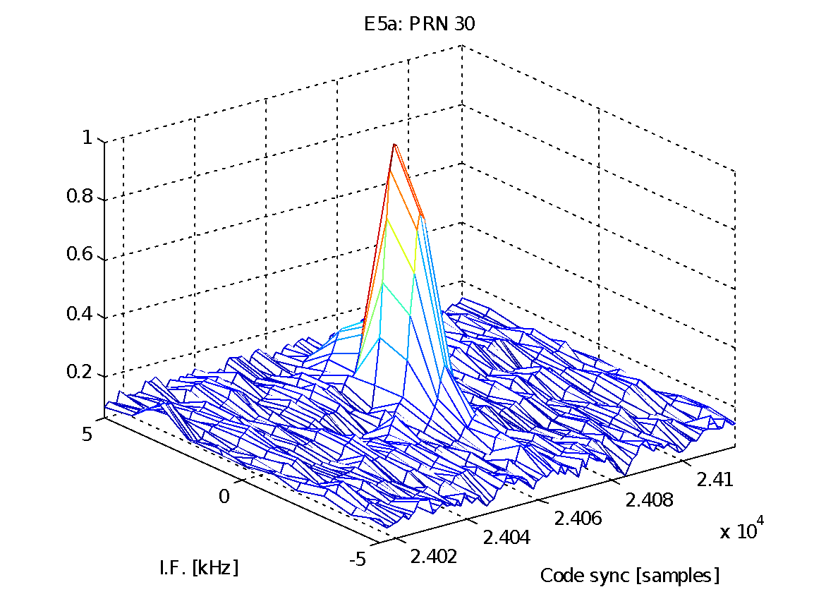 |
Figure 13: E5a acquisition of E30
 |  |
Figure 14: E5b acquisition of E30, showing a perfect match in code delay with E5a as one would expect.
Conclusions and work to do
I am very suprised of how little time took me from unboxing the kit to sucessfully using it to acquire all the GNSS signals I could think and test all configurations. Of course I had the former experience with the NT1036 but this time I had the perception of a solid, feature-rich, plug-and-play IC.
In my todo list there is the extension of this post with a home-made measurement of channel isolation.. and the way I plan to do it should be interesting to the readers :)

23 comments:
What is the cost of the evaluation board?
I don't know, please ask NTLab. I understand that SwiftNav is building on the NT1065, so perhaps the next version of Piksi (expected for this fall) will be usable as evkit too. Cheers, Michele
Hi Michele,
I am thinking of buying the evaluation board of NT1065. I am not very convinced about the 2 bit ADC. How was your experience with getting the digital data from analog? Is the resolution good enough for further baseband processing? Is there a way to integrate a high resolution ADC with the eval board? Thank you for your response.
Well I only used the internal ADC converter of the NT1065 which worked really well for me. In fact, 2 bit samples guarantee virtually no loss in presence of AWGN only. Noisy environment would benefit more bits but it all complicates quite a bit. You can integrate a high resolution ADC with the evaluation kit: you will need to mount baluns and use the analogue output of the NT1065. Sharing the clock between the evkit and ADC would be wise. I suggest you contact NTLab if you are going to try tweaking to this level.
Thank you very much :)
What exactly is the output of the board? Is it the digitized samples of demodulated gps signal or is it the NAV data (baseband processed samples)?
Now I am not sure anymore you understood my blog post..
The output of the NT1065 evaluation kit if digitized samples.
Hi,
NT1065 or NT1036 are new Front-End chips from unknown factory. what is your opinion about these chips? can I use these chips for implementing reliable GNSS receivers?
Best Regards
What an odd comment..
If I answer "no" I will unmotivatedly cast doubts over the seriousness of NTLab as fabless chipset design Company.
If I answer "yes" I will take full responsibility over your next build of "reliable" GNSS receivers.
So I guess I shall not answer.. or rather do with another question "are you an entrepreneur?"
Hi,
I know my question was silly. Yes,I am an entrepreneur. Can you introduce me some front-end chips to receive gps/glonass signal? What is your opinion about max2769? I had some problem with it.
Many thanks for your assistance
I know the MAX2769 well: it will not do GPS and Glonass simultaneously. I did not have issues worth mentioning though, what about yours?
For GPS+Glonass you need something like the CAN5125 or the XN116 (just google them). The NTLab NT1065 belongs to a new generation (not from 8 years ago as the MAX2769) and allows doing things that 4 individual MAX2769s won't. Please refer to the datasheets, and match characteristics with your actual needs.
Hello Michele,
We are trying to interface NT1065 with Zynq FPGA, NT1065 is powered by 3V and (Zynq FPGA)Bank 34 in Zynq 7020 SoC by 3.3V, I mean we are configuring NT1065 registers using SPI interface from Zynq FPGA, will it work with 3.3V?
Because this is still under design stage
Please guide us
Well, I think this has little to do with the NT1065 specifically.. I am not a super expert, but although it is always advisable to run both ends of a logic line with the same voltage, small differences in voltage are possible. Usually a small resistor takes care of limiting the currents involved in the voltage drop and also acts as a useful decoupling element for digital noise and/or return signals (which you might want indeed between a FPGA and a GPS front-end). Sometimes for better de-coupling you might even want to add a small capacitor in a RC configuration. Knowing nothing about your design, I'd mention that I have seen 33 ohm used in those cases in the past.
Also remember to check in the Zynq driver datasheet that the minimum valid input logic high level is well above 3V (usually it's 0.8*V - if that's the case you should be OK)
Hi Michele,
Thank You for your guidelines, if there is anything else I'll get back to you...
Hi...
I'm Interfacing NT1065_FMC Evaluation Kit with Zedboard (source code provided by NT labs) in this through Xilinx chipscope acquiring data and using Matlab source code plotted spectrum (db Vs Frequency) the spectrum shows some peaks at 4.999Mhz and power level 139.3 dB, so is this correct data we are acquiring.(actually the data file provided by NT Labs Gives peaks at 6.001 Mhz and power level 71.87dB)
Also our aim is to acquire real time raw data from NT1065_FMC Evaluation Kit and process it using FPGA/ Using MATLAB so please suggest us a method.
As you tested NT Board in Jan 2016, at that time you used USB DAQ FX2LP for testing, In the same way we wanted to test it using FPGA will it be possible so please guide us.
Thanks & Regards
Navnath Chikhale
Hi Michel,
As I tried with NT1065 Evaluation Kit using Zedboard, When I ported out Mag and Sign data (NT1065 Internal ADC output) to one of PMOD connector of Zedboard, it gives us Digital Output, but when we removed Antenna (GPS L1)from channel-1 still the same signals observed on DSO (no change), so please guide me How to capture actual and real data. If possible please suggest processing of raw data in FPGA.
As well I ported out Clock from NT1065 it gives us perfect Output on DSO.
Observation In NT GUI:
RF Gain: 25.3 dB, IF Gain: 16.6 (when we removed Antenna its showing: 50.3 dB)
Status: Calibration Ok- Green,
AOK- Green,
Settings selected as follows
TCXO-10MHz,
Channel-1 selected
PPL-A
IF pass Band-30.10MHz
2-bit ADC Output,
RF AGC- Manual
IF AGC- Auto
N-Divider-159
R-Divider-1
Mah.. I am not a consultant to you guys.. that seems a little specific for a blog comment.
I don't know the specifics of the FMC evaluation kit.. so it's a little hard to guess what you should be expecting.
Anyway, is the antenna an active antenna?
If no, you'd expect no difference when plugging it in and out of a channel input.
If yes, did you use a bias-tee to power it up?
For FPGA code I'd say my friend Takuji has good references:
http://blog.goo.ne.jp/osqzss/c/e089caedb72f1a5b9e8ff6160b84ecc9
Thanks for Reply,
Yes I'm using Active Antenna, the on board (NT1065 Evaluation Kit) bias tee is used for power up.
Can you give the part no of the TCXO used on this board.
Dear Michele Bavaro
I am working on the gnss interfrence mitigation ,please can you help to get the data with jammer for my simmulation..
kind regards
Sir,
I am using this card and when i set the local oscillator frequency to 1170 for receiving IRNSS L5 band @ 1176.4 MHz iam getting an IF frequency at 8.85 MHz instead of 6.4MHz. what could be the problem.
When I connected my NT1065 with the acquisition and tracking hardware in FPGA in the acquired code phase there is a random shift then we observed the sampling clock of NT1065 through spectrum analyser we noticed the sampling clock is changing ie not giving stable output. Kindly suggest what would be the problem. Is there any stability problem in the NT1065 RF board
Post a Comment